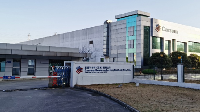
Carsem Semiconductor (Suzhou) Co., Ltd.
The facility covers a total construction area of approximately 15,000 square meters, including a 9,200-square-meter Class 10,000 cleanroom. By focusing on advanced packaging technologies, the project upgrades CSP processes and introduces flip-chip bonding techniques to overcome bottlenecks in wide bandgap semiconductor packaging, achieving micron-level precision. Integrated with smart equipment and digital systems, production efficiency has been significantly enhanced.
2021-03-05
More